Don't miss our holiday offer - up to 50% OFF!
5in1 DIY Soldering Practice Kit Large USA Flag, SOP8 Chip Practice Board, CD4017 Green, 0603 Red & 0606 Blue SMD/SMT Kits for Beginners & Soldering Skill Mastery Let You Master Welding Skills


Price: $69.99 - $29.76
(as of Jun 15, 2025 02:55:19 UTC – Details)
Product Description


This LED circuit board with an American theme is a creative work that combines patriotism with technology. On its front side, referring to the American flag, the LED lights are arranged to form the pattern of the American flag, accompanied by the words “God Bless America”. On the back side, the letters “USA” and the words “The American Flag Will Never Fall” are prominently presented, and the Independence Day of the United States, “July 4, 1776”, is marked on the back as well.
The circuit board is made of 1.6-millimeter-thick international standard board materials, with the pads tinned, making it both sturdy and having good electrical conductivity. The LED lights possess the characteristics of high brightness and low power consumption, and can emit bright and uniform light.
It has a wide range of application scenarios. When used for home or office decoration, it can create a unique atmosphere, and it is also quite attractive in commercial places. Electronics enthusiasts and engineers can also apply it to the development of electronics projects. With an appropriate size, a large number of components and a standard working voltage, it is undoubtedly a creative product worth having.
1、PCB board size: 68 × 108 mm
2、PCB board thickness: 1.6 mm
3、PCB material: International standard board, all solder pads are tin plated, high-strength material.
4、The working voltage of the circuit is DC 3 – 5V.
5、Number of components: 772
6、Number of solder joints: 1544
7、Function/Feature: RGB LED USA Flag (L)
8、Sample welding time: Approximately 140 minutes.

After the surface-mount components are soldered, power is applied to form a running light effect to test the soldering quality. When power is just turned on, since the voltage across capacitors C1 – C9 cannot change suddenly, pin 2 of the NE555 is at a low level and the output pin 3 is at a high level. When the power supply charges C1 – C9 through R6, R70, RP1 – RP5 until the voltage across C1 – C9 reaches two-thirds of the power supply voltage, the level of output pin 3 changes from high to low. The internal circuit of the NE555 becomes conductive, and capacitors C1 – C9 discharge through pin 7 of the NE555. Until the voltage across C1 – C9 drops below one-third of the power supply voltage, the level of pin 3 of the NE555 changes from low to high again, and C1 – C9 is charged once more, thus forming a cyclic oscillation. Changing the values of RP1 – RP5 can alter the output frequency of the oscillator. The clock oscillation signal of the NE555 is continuously applied to pin 14 of the 4014. There are ten transistors connected to the ten output pins of the 4017 to drive ten LEDs. Under the action of the clock signal, the ten output pins of the 4017 alternately generate high levels, so that L1 – L10 are lit up one by one, forming the running light effect.
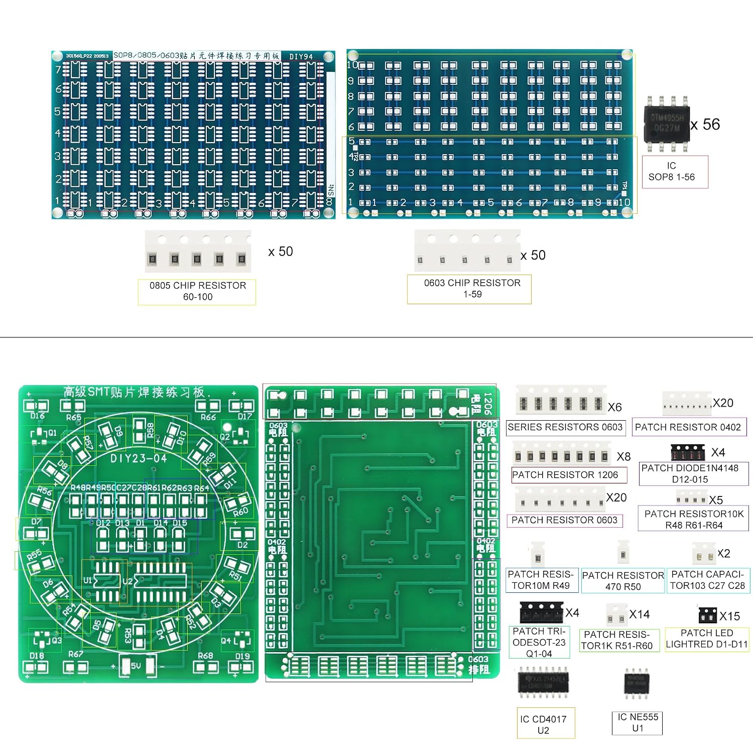
1、PCB board size: 70 × 57 mm
2、PCB board thickness: 1.6 mm
3、Board material: International standard board material, all solder pads are tin-plated, high-strength material.
4、Circuit working voltage: DC 5V
5、Number of components: 149
6、Number of solder joints: 444
7、Function/Characteristic: IC SOP8
8、Sample welding time: Approximately 65 minutes

This circuit is an application circuit of NE555 + 4017. The NE555 forms a multivibrator, and the pulse oscillation signal is output from pin 3 of the NE555 to the CD4017 for counting. The CD4017 will sequentially output high levels on Q0 – Q9 along with the input pulse signals to light up the corresponding light-emitting diodes. These light-emitting diodes are arranged in a circle to form the effect of running lights. When the CD4017 finishes counting up to 10, the carry terminal C0 changes from low to high to drive the transistors Q1 – Q4 to conduct, thus lighting up the light-emitting diodes at the four corners. After the next pulse arrives, the C0 terminal returns to a low level, and the light-emitting diodes at the four corners are turned off. This cycle repeats.
PCB board size: 58 × 47 mmPCB board thickness: 1.6 mmBoard material: International standard board material, all solder pads are tin-plated, high-strength material.Circuit working voltage: DC 5VNumber of components: 92Number of solder joints: 244Function/Characteristic: Circulate Flash Red LEDSample welding time: Approximately 40 minutes

In order to improve the soldering skill levels of electronics major students and electronics enthusiasts, referring to the packaging types of surface-mount components in the Electronics Product Assembly and Debugging Skills Competitions of national vocational colleges in recent years, this surface-mount soldering practice board has been specially designed with the intention of enhancing the soldering level and speed.
1、PCB board size: 84 × 60 mm
2、PCB board thickness: 1.6 mm
3、Board material: International standard board material, all solder pads are tin-plated, high-strength material.
4、Circuit working voltage: DC 5V
5、Number of components: 110
6、Number of solder joints: 326
7、Function/Characteristic: 0603 series resistors
8、Sample welding time: Approximately 45 minutes

In order to improve the soldering skill levels of electronics major students and electronics enthusiasts, referring to the packaging types of surface-mount components in the Electronics Product Assembly and Debugging Skills Competitions of national vocational colleges in recent years, this surface-mount soldering practice board has been specially designed with the intention of enhancing the soldering level and speed.
1、PCB board size: 84 × 60 mm
2、PCB board thickness: 1.6 mm
3、Board material: International standard board material, all solder pads are tin-plated, high-strength material.
4、Circuit working voltage: DC 5V
5、Number of components: 100
6、Number of solder joints: 306
7、Function/Characteristic: 0603 series resistors
8、Sample welding time: Approximately 45 minutes

Package Dimensions : 2 x 2 x 2 inches; 6.4 ounces
Item model number : YIDAB005
Date First Available : February 28, 2023
Manufacturer : Yidab
ASIN : B0BX2QST6M
Country of Origin : China
Unbeatable 5 – in – 1 Value Get a premium bundle including a Large USA Flag kit, SOP8 Chip Practice Board, and three SMD/SMT kits (Green CD4017, Red 0603, Blue 0606). Enjoy diverse projects at one great price—ideal for expanding soldering expertise.
Perfect for All Skill Levels Whether a beginner or enthusiast, these kits help master soldering. From learning basics to tackling advanced SMD/SMT tasks, unlock creativity and skill growth.
Superior Quality Components Each kit features high – grade materials for reliable performance and long – lasting results. Ensure smooth soldering and durable, professional – looking creations.
Versatile Applications Ideal for home decor, educational use, or gifts. Create striking displays (like the Large USA Flag) or functional electronics—endless possibilities for every occasion.
Exceptional Customer Support Our team is dedicated to your satisfaction. Have questions or need help? Reach out for prompt, friendly assistance—we’re here to enhance your experience.